Suhir E and Ghaffarian R
A previously developed analytical thermal stress model is used for the assessment of the effect of the glasstransition
temperature (Tg) of the underfill encapsulant and the thickness of the underfill-solder composite bond (USCB)
on the induced stresses. The calculations were carried out for two Tg levels, above and below the operation and testing
temperature range for the flip-chip (FC) or the fine-pitch ball-grid-array (FPBGA) assembly with an USCB, and for two
thicknesses, 0.05 mm and 0.1 mm, of the USCB. Calculations indicated that the Tg level of the underfill material had a
significant effect on the induced stresses: the normal stresses in the USCB with a low-modulus (low Tg) underfill were
about half the stresses of the design with high-modulus (high Tg) underfill, and this was true for both thin (0.05 mm
thick) and thick (0.1 mm thick) USCB layers. As to the role of the USCB thickness, thicker USCBs exhibit somewhat
lower normal stresses, than thin layers, but the effect is insignificant. The maximum predicted shearing stresses occur
at the USCB/chip, and not at the USCB/substrate interface. This result is in agreement with the observed, in a number
of experiments, delaminations at the USCB/chip interface, and not at the USCB/substrate interface. The obtained data
indicate also that (in a way, contrary to the current practice) there is an incentive for using low Tg underfills, provided, of
course, that their adhesive strength is proven to be sufficient for the lower stress level. This is an important requirement,
of course, and might explain why electronic product manufacturers employ mostly high Tg underfills. As to the incentive
for using thicker USCBs, the increase in this thickness from 0.05 mm to 0.1 mm resulted in a minor relief in the normal
stress in the USCB for both high and low Tg underfills, but led to an appreciable relief in the interfacial stresses at the
USCB/chip interface, especially for high Tg underfills: the predicted stress relief in this case was as significant as 34%.
For low Tg underfills the stress relief was much lower, but still appreciable: about 19%. Thicker USCB layers could be
more effective, because, as has been shown in our earlier publications and confirmed experimentally, elevated stand-off
heights of solder joint interconnections are able to provide appreciable stress relief in the solder material by making the
bonding system more compliant. Indeed, for the thickness of 0.75 mm (impossible for FC designs, but rather typical for
FPBGA systems) the decrease in the normal stress acting in the USCB cross-sections is appreciable, and the decrease
in the shearing stress at the USCB/chip interface is as high as 70% in the case of high Tg underfill and even higher, 76%,
in the case of low Tg underfill. The employed analytical stress model used in this analysis can be used for the selection
of the adequate underfill material and establishing the appropriate USCB thickness at the design stage. It is noteworthy
that, as long as the linear approach is used and the induced stresses are proportional to the change in temperature, the
developed model can be used also in situations, when the underfill’s Tg is between the temperature extremes that the
assembly of interest experiences during its accelerated testing and in actual operation conditions.
Share this article
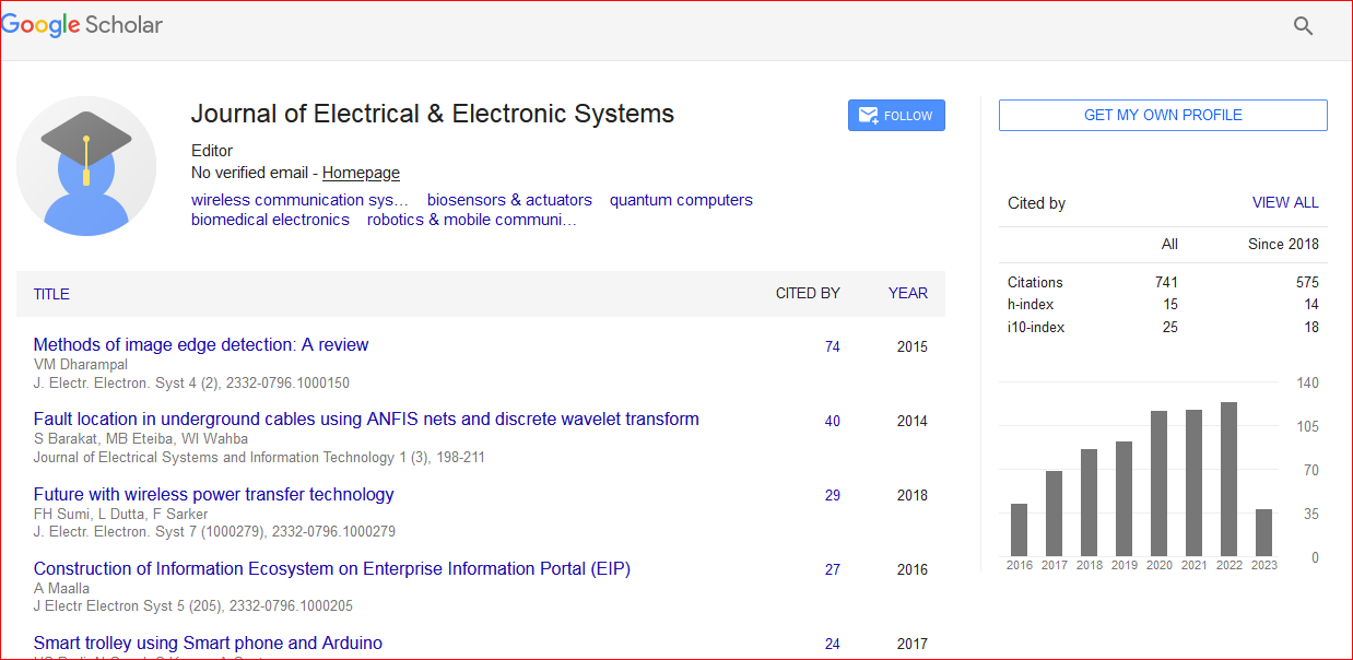
Journal of Electrical & Electronic Systems received 733 citations as per Google Scholar report