Perspective - (2022) Volume 13, Issue 12
Received: 03-Dec-2022, Manuscript No. CSJ-23-90618;
Editor assigned: 05-Dec-2022, Pre QC No. P-90618;
Reviewed: 19-Dec-2022, QC No. Q-90618;
Revised: 24-Dec-2022, Manuscript No. R-90618;
Published:
30-Dec-2022
, DOI: 10.37421/2150-3494.2022.13.327
Citation: Onkar, Rami. “Study of SiO2 Etching using Plasma Diagnostics.” Chem Sci J 13 (2022): 327.
Copyright: © 2022 Onkar R. This is an open-access article distributed under the terms of the Creative Commons Attribution License, which permits unrestricted use, distribution, and reproduction in any medium, provided the original author and source are credited.
Plasma is described as semi-neutral plasma of charged, unbiased particles that exhibits collective behaviour. The distinctive features that distinguish plasma from other release characteristics are applied in many contemporary and research sectors, such as regulating the component particles for specific uses.
Plasma • Nuclear • SiO2
Plasma has distinctive physical and chemical properties depending on the electron thickness and temperature systems, resulting in a different classification of plasma including material handling plasma and combination plasma [1]. Plasma has a huge range of electron densities and temperatures, which are the most delegate boundaries. Material handling has grown into one of the most important sub-fields of low temperature plasma, which is designated as such by its electron temperature system [2] because to the rapid development of the semiconductor industry in the twentieth century. Low temperature plasma is widely used in the fundamental semiconductor fabrication cycles, such as scratching, testifying, cleaning, and so on. This allows plasma to play a significant role in the microelectronics industry.
To meet market demands, however, further advancement of electronic devices necessitates increasingly improved plasma processes, increasing the handling difficulty and complexity. In this case, plasma diagnostics can provide arbitrary and objective information on plasma borders to help understand the physical and chemical peculiarities in plasma processes, which will promote plasma innovation [3].
The cycle window, which may be defined as the state of the handling equipment or plasma itself that must be satisfied to comprehend the reason for the interaction, can be laid out by plasma handling architects with the assistance of inner plasma boundaries obtained by plasma diagnostics. For instance, SiO2 scratching using Fluorocarbon plasma anticipates that plasma particles be significant areas of strength for sufficiently, the FC plasma would frame thick FC films on the SiO2 instead of cutting it. Another model can be found in the unique plasma process known as nuclear layer testimony, where a specific temperature window is necessary to acknowledge a nuclear scale statement without deforming the delivery of synthetic responses, such as buildup or desorption at temperatures beneath or above the window, separately.
Fundamentally, nuclear layer scratching (ALE), the partner of ALD, also has a recognisable interaction window for the appropriate particle energy range that achieves nuclear scale expulsion without deformity producing actual reactions, such as inadequate evacuation or faltering at particle energies underneath or over the window, separately [4]. There are numerous reports on the plasma diagnostics' display using various methods to achieve the interaction window. Some plasma cycles, such as ALE, where at least two types of plasma are rotated gradually, as opposed to consistent plasma processes where single plasma is maintained throughout the handling period, may benefit especially from plasma diagnostics.
One prior study includes a thorough analysis of the release material science of ALE plasma, covering everything from release shakiness and recovery times during the ALE cycle to a few key plasma boundaries, such as electron thickness and temperature [5]. This study uses plasma diagnostics to investigate a cycle window change in SiO2 scratching with FC plasma from a variety of information power. The devices used in this study are painstakingly evaluated for their compatibility with the FC plasma's polymeric states. This work views the FC revolutionary thickness as the boundary displaying the FC extremist motion in light of a previous study that found a consistent condition of drawing still in the air by the harmony between FC film statement and SiO2- FC film expulsion rates, which are separately reflected by FC extremist and particle energy transitions.
Plasma demonstration tactics have a bigger role in understanding and managing handling plasma for better results now that it is widely used in material handling. The cycle window shift, which occurs when an increase in RF power pushes the handling state through the window, was investigated in the current work using various plasma demonstration approaches.
The target species for the diagnostics of electron thickness, plasma potential, and FC extreme densities were chosen in light of the previously published detailed SiO2 scratch model. The obtained demonstration results were in perfect agreement with the engraving model anticipation and had the capacity to make sense of the cycle window change.
It is important to note that the repercussions of plasma processes, as shown in this work, are easier to understand when different analytic instruments are used to screen similar plasma. Finally, in situ plasma demonstration approaches are anticipated to provide more relevant analytic outputs for some perplexing plasma processes, such as ALE where plasma gradually varies throughout the cycle, allowing for more precise and proper interaction controls.
None.
None.
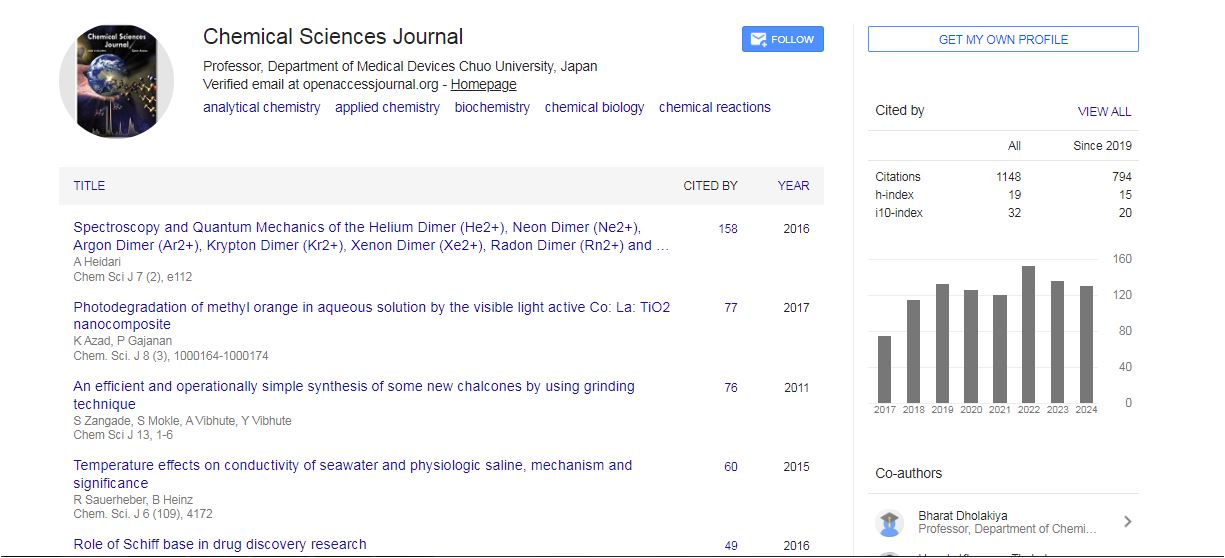
Chemical Sciences Journal received 912 citations as per Google Scholar report