Norbert Janik, Pawel Scharoch and Robert Kudrawiec
Wroclaw University of Science and Technology, Poland
Scientific Tracks Abstracts: J Astrophys Aerospace Technol
Materials composed of the group IV elements are promising candidates for designing the nano-optoelectronic
devices integrated with Si based circuits. Special requirements concerning the electronic properties of the
materials (direct band-gap, high mobility of carriers) can be met via the electronic structure engineering. One of
methods of modifying the electronic structure is applying the strain [1, 2, 3], e.g. by the choice of unmatched lattices
in epitaxial technologies. In this work the DFT based computational methods have been applied to investigate
systematically the effect of strains on electronic structure, with the use of ABINIT program. In reference to available
technologies the isotropic as well as uniaxial and biaxial strains for crystallographic planes (100), (110) and (111) in
diamond like crystals of C, Si, Ge and Sn have been studied. The systems were strained in the range of +/�??4%. The
following characteristics have been evaluated as functions of the strain: Poison�??s ratios, elastic coefficients, band gaps
in between chosen band structure points and band offsets. A detailed discussion of observed effects (considering
also the orbital composition of bands) such as indirect direct gap transition, opening/closing the gaps, strain induced
symmetry breaking effect and band offsets, the effect of lowering the band gap on electron mobility, will be presented.
Recent Publications
1. Polak M P, Scharoch P and Kudrawiec R (2017) The electronic band structure of Ge1�??x Sn x in the full
composition range: indirect, direct, and inverted gaps regimes, band offsets, and the Burstein�??Moss effect.
Journal of Physics D: Applied Physics 50.19:195103.
2. Polak M P, Scharoch P and Kudrawiec R (2015) First-principles calculations of bismuth induced changes in the
band structure of dilute Ga-V-Bi and In-V-Bi alloys: Chemical trends versus experimental data. Semiconductor
Science and Technology 30(9):094001.
3. Kopaczek J, Polak M P, Scharoch P, Wu K, Chen B, Tongay S, et al. (2016) Direct optical transitions at K- and
H-point of Brillouin zone in bulk MoS2, MoSe2, WS2, and WSe2. Journal of Applied Physics 119(23):235705.
4. Dyba�?a F, Polak M P, Kopaczek J, Scharoch P, Wu K, Tongay S, et al. (2016) Pressure coefficients for direct optical
transitions in MoS2, MoSe2, WS2, and WSe2 crystals and semiconductor to metal transitions. Scientific reports
6:26663.
5. Kudrawiec R, Kopaczek J, Polak M P, Scharoch P, Gladysiewicz M, Misiewicz J, et.al. (2014) Experimental and
theoretical studies of band gap alignment in GaAs1-xBix/GaAs quantum wells. J Appl Phys; 116(23).
Norbert Janik is a PhD student at Theoretical Physics Department and has his expertise in ab initio calculations of strained systems.
E-mail: norbert.janik@pwr.edu.pl
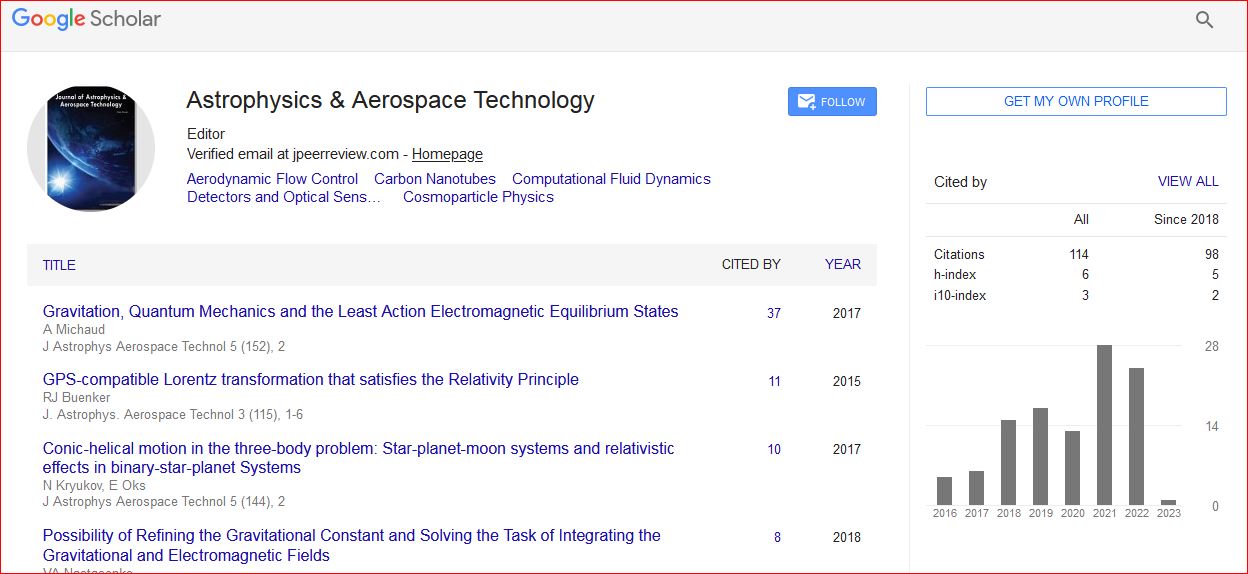
Astrophysics & Aerospace Technology received 114 citations as per Google Scholar report

 Spanish
  Chinese
  Russian
  German
  French
  Japanese
  Portuguese
  Hindi
Hindi 